How are solar panels made?
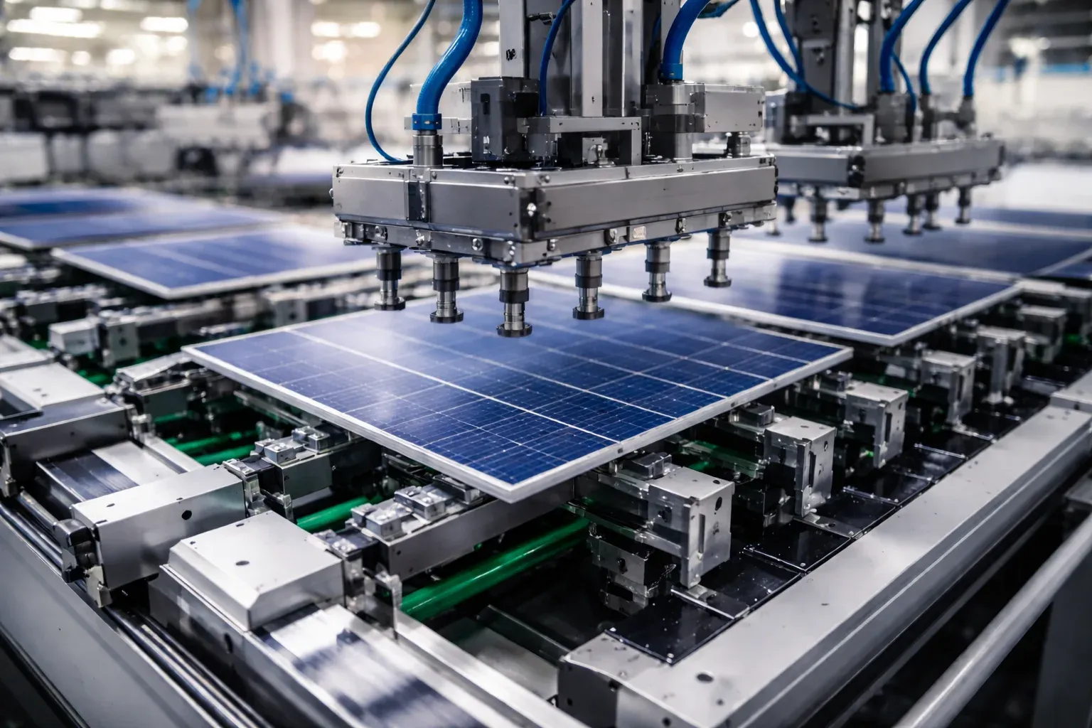
Solar panels convert sunlight into electricity, primarily using semiconductor materials like silicon. The manufacturing process transforms raw silicon into highly pure ingots, which are then sliced into wafers and processed into individual solar cells. These cells are then assembled into modules, encapsulated for protection, and framed to create the finished solar panel. While manufacturing is energy-intensive, solar panels typically generate significantly more clean energy over their lifespan than is consumed during their production.
Understanding the journey of solar panels from raw materials to energy-producing devices can help you make informed decisions about your home's energy choices.
The journey from sand to solar power
Solar panels, a cornerstone of renewable energy, seem like complex technology, but their creation begins with one of Earth's most abundant elements: sand. The journey from simple quartz sand to a high-efficiency solar panel involves a precise, multi-step manufacturing process that transforms raw materials into devices capable of converting sunlight into usable electricity.
Key materials: what goes into a solar panel?
Solar panels are primarily composed of a few key materials, each playing a crucial role in their function and durability.
Silicon: the heart of the solar cell
Silicon is the most common semiconductor material used in solar cells, accounting for over 90% of the market share. It is the active component that converts sunlight into electricity through the photovoltaic effect. Silicon is derived from quartz sand, which is abundant globally. The purity of the silicon directly impacts the efficiency and lifespan of the solar cell.
Glass, aluminium, and other components
Beyond silicon, solar panels incorporate several other materials:
- Glass: Typically tempered glass, it forms the front layer, protecting the delicate solar cells from environmental elements like rain, hail, and dust.
- Aluminium: An aluminium frame surrounds the module, providing structural integrity, protection, and ease of mounting.
- Encapsulant material: Layers of ethylene vinyl acetate (EVA) film are used to encapsulate the solar cells, bonding them to the glass and backsheet while protecting them from moisture and vibration.
- Backsheet: A protective backsheet, often made of plastic, shields the rear of the solar cells from moisture and degradation.
- Metal contacts: Thin metal contacts (often silver or copper) are printed onto the cells to collect the electrical current generated when sunlight strikes the silicon.
- Junction box: Located on the back of the panel, the junction box houses the electrical wiring and bypass diodes, facilitating the connection of panels into a solar array.
The solar cell manufacturing process: step-by-step
The creation of a solar cell is a meticulous process, starting with raw silicon and ending with a highly efficient energy-converting device.
Silicon purification and ingot formation
The first step involves purifying silicon from quartz sand to create metallurgical-grade silicon. This requires heating the sand with carbon in industrial furnaces to temperatures exceeding 2,000°C, which removes oxygen and leaves behind impure silicon. This metallurgical-grade silicon is then further refined through chemical processes to achieve extremely high purity levels, often exceeding 99.9999% (known as "6N" purity), essential for efficient electron movement in solar cells.
Once purified, the silicon is melted and formed into large, solid blocks called ingots. For monocrystalline panels, a single crystal ingot is grown slowly from molten silicon, ensuring a uniform atomic structure. For polycrystalline panels, molten silicon is cast into blocks and allowed to cool naturally, resulting in multiple silicon crystals.
Wafer slicing and cell processing
The silicon ingots are then sliced into extremely thin wafers, typically thinner than a millimetre, using precision wire saws. This slicing process is highly precise, though it can result in some silicon loss as "kerf" (sawdust). After slicing, the wafers are polished, cleaned, and inspected for defects.
Next, the wafers undergo texturing, where their surface is lightly roughened to reduce reflectivity and enhance light absorption. This creates pyramid-like structures that trap more sunlight.
Adding contacts and anti-reflective coatings
To create the p-n junction necessary for the photovoltaic effect, the wafers are "doped" with specific chemicals. One side is doped with phosphorus to create a negative charge, and the opposing side with boron for a positive charge. This junction allows electrons to flow in a specific direction when exposed to light.
An anti-reflective coating is then applied to the wafer surface. This coating minimises light reflection, ensuring that more sunlight is absorbed by the silicon to generate electricity. Finally, thin metal contacts are screen-printed onto the front and back of the cells to collect the electrical current.
Assembling the solar panel module
Individual solar cells are not a panel; they must be carefully assembled into a module to create the finished product.
Connecting cells and encapsulation
Once the individual solar cells are manufactured, they are interconnected, typically by soldering them together in a series to form strings. These strings are then laid out on a sheet of tempered glass. Layers of ethylene vinyl acetate (EVA) encapsulant are placed above and below the cell strings, and a protective backsheet is added to the bottom.
This layered assembly is then laminated under heat and vacuum. This process permanently bonds all the layers together, creating a sealed, weather-resistant module that protects the sensitive cells from moisture, dirt, and physical damage, ensuring long-term performance.
Framing and quality control
After lamination, an aluminium frame is attached around the edges of the module. This frame provides structural support, protects the edges of the laminated layers, and simplifies mounting the panel onto a roof or other structure. A junction box is then installed on the back of the panel, providing the electrical connection points for wiring the panel into a solar array.
Finally, each finished solar panel undergoes rigorous quality control and testing. This includes electrical performance tests (often using an "artificial sun") to verify power output and ensure it meets specifications, as well as checks for any defects or micro-cracks not visible to the naked eye.
Different types of solar panels and their production
While the basic principles remain, variations in manufacturing lead to different types of solar panels with distinct characteristics.
Monocrystalline vs polycrystalline panels
The primary distinction lies in the silicon used:
- Monocrystalline panels: These are made from a single, continuous silicon crystal, grown using the Czochralski process. This uniform structure allows electrons to move more freely, resulting in higher efficiency, typically between 20-23%. Monocrystalline panels often have a sleeker, darker appearance and perform better in warmer temperatures. They are generally more expensive but require less space to generate the same amount of electricity.
- Polycrystalline panels: These are made by melting multiple silicon fragments together and casting them into a block, resulting in multiple crystals. The presence of grain boundaries between these crystals reduces electron mobility, leading to slightly lower efficiencies, usually between 15-18%. Polycrystalline panels are typically more budget-friendly and have a bluer, speckled appearance.
What is the efficiency difference between monocrystalline and polycrystalline solar panels?
Monocrystalline solar panels typically offer higher efficiency, ranging from 20-23%, due to their single-crystal silicon structure. Polycrystalline panels, made from multiple silicon crystals, usually have efficiencies between 15-18% and are generally more budget-friendly.
Thin-film solar technology
Thin-film solar panels use different semiconductor materials, such as cadmium telluride or amorphous silicon, deposited in thin layers onto a substrate like glass or plastic. This manufacturing process differs significantly from crystalline silicon panels. Thin-film technology is generally more flexible and lighter, but it typically has lower efficiency compared to crystalline silicon panels, making it less common for residential rooftop installations where space is often a constraint.
Understanding the environmental footprint
The manufacturing of solar panels, particularly the purification of silicon, is an energy-intensive process. However, it is crucial to consider the long-term benefits. Solar panels typically generate significantly more clean energy over their lifespan than is consumed during their production. The energy payback time for solar panels - the time it takes to generate the energy equivalent to that used in their production - is generally between 6 and 14 years in the UK.
The average lifespan of a modern solar panel is typically 25 to 30 years, with many continuing to produce electricity beyond this period. This means that for the vast majority of their operational life, solar panels are producing clean, renewable energy, offsetting the initial energy investment and contributing to a more sustainable energy system.
Making the most of your solar investment with Fuse Energy
Understanding how solar panels are made highlights their potential for abundant, clean energy. For UK homeowners, having solar panels is just the first step; intelligently managing the energy they produce is key to maximising their benefits.
While Fuse does not install solar panels, we help you manage the abundant energy your panels generate through smart tariffs and an intuitive app. Our smart tariffs are designed to help stabilise the grid and optimise your energy usage, aligning with our vision of a future with 'power to play with'. This approach aligns with our vision of enabling you to use more energy and manage that abundance effectively within your home energy system.
Managing your home's energy, especially with solar panels, should be straightforward. Fuse Energy offers clear pricing and an intuitive app to help you track your usage and make the most of your generated electricity. Our 24/7 human support team is always available to assist you.
Disclaimer
For the avoidance of doubt, this article is provided for informational purposes only and is not intended to constitute legal or financial advice. The author and/or Fuse Energy shall not be responsible for any losses arising out of any reliance on the information contained herein.